Next-generation memory devices with reduced power consumption
A technology developed in Japan could enable electric-field-based data writing into memory devices with reduced energy consumption.
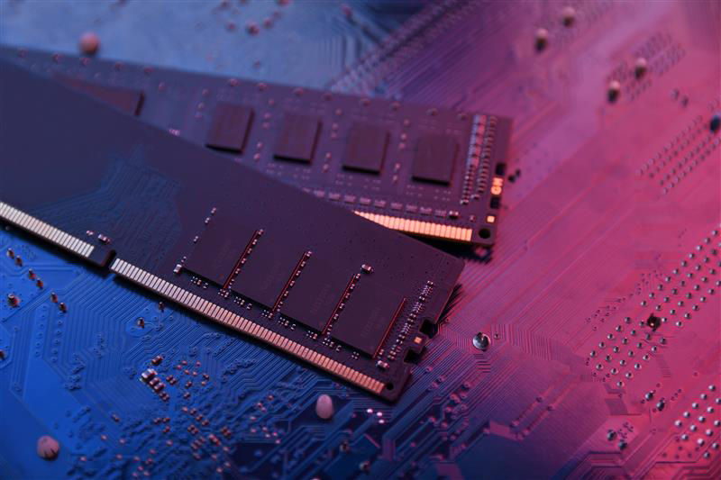
This could boost the development of next-generation magnetoresistive random access memory (MRAM) devices.
MRAM offers several advantages over conventional random access memory (RAM), including non-volatility, high speed, increased storage capacity and enhanced endurance.
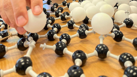
MRAM, for example, does not use capacitors for its basic storage units, which produce a volatile charge stage. Instead, non-volatile data storage comes from its use of magnetic states, namely the orientation of magnetisation.
This memory type also provides low-power consumption in the standby state, but previously had challenges with its energy consumption during data writing. This is because MRAM devices typically require a large electric current to switch the magnetisation vectors of magnetic tunnel junctions during the writing process. This leads to Joule heating and, consequently, unwanted power consumption.
Now, researchers at Osaka University claim to have developed a component for MRAM that overcomes this issue.
They concluded that an energy-efficient data writing scheme could be achieved using a multiferroic heterostructure with magnetisation vectors that can be switched by an electric field. However, before these materials can be inserted into spintronic memory devices, two requirements must be met, explains lead author Takamasa Usami.
The first is to achieve a giant converse magnetroelectric (CME) effect, which characterises the heterostructure’s response to an electric field, with larger values indicating stronger magnetisation.
A paper on Giant converse magnetoelectric effect in a multiferroic heterostructure with polycrystalline Co2FeSi in NPG Asia Materials, reveals how a combination of a cobalt (Co)-based Heusler alloy, Co₂FeSi, and piezoelectric PMN-PT exhibits a large CME coupling coefficient of more than 10-5s/m. Consequently, a 'steep change in the magnetisation direction was achieved by applying an electric field', says Usami.
The second requirement is to achieve a non-volatile binary state at zero electric field. In other words, the two magnetic states that correspond to binary data of 0 and 1 can be retained after the electric field is switched off, says Usami.
Originally, the Osaka researchers fabricated multiferroic heterostructures that consist of Co2FeSi/ultra-thin Fe/PMN-PT layers using a molecular beam epitaxy.
The issue here, Usami explains, is that an amorphous layer forms at the interface between the ferromagnetic and piezoelectric layers, which hinders a reliable electric field.
They have resolved this issue by substituting the ultra-thin, iron-based layer with a vanadium atomic layer, which is inserted between the ferromagnetic and piezoelectric layers to improve the interface’s stability and its crystal quality.
By changing the electric field sweeping operation, the researchers have demonstrated how two different magnetic states can be reliably realised at zero electric field. Also, they state the CME effect reaches a larger value than without a vanadium layer.
'The vanadium layer provides a clear interface, resulting in a highly oriented ferromagnetic Co₂FeSi layer,' says Usami. 'Due to the improvement of the crystal orientation of the Co2FeSi layer, finally, we intentionally tune the magnetic anisotropy with reproducibility. As a result, it enables us to obtain reliable non-volatile binary state at zero electric field.'
Further work is required to fabricate the piezoelectric layer into a thin film before insertion into MRAM devices.
To develop magnetoelectric (ME)-MRAM devices, the team plans to study the performance of a heterostructure that contains both magnetic and piezoelectric thin films.