Hexagonal boron nitride substrates for graphene-based electronics
Dr Michael Ford MIMMM at Haseltine Lake Kempner explores a patent relating to hexagonal boron nitride on silicon-based substrates.
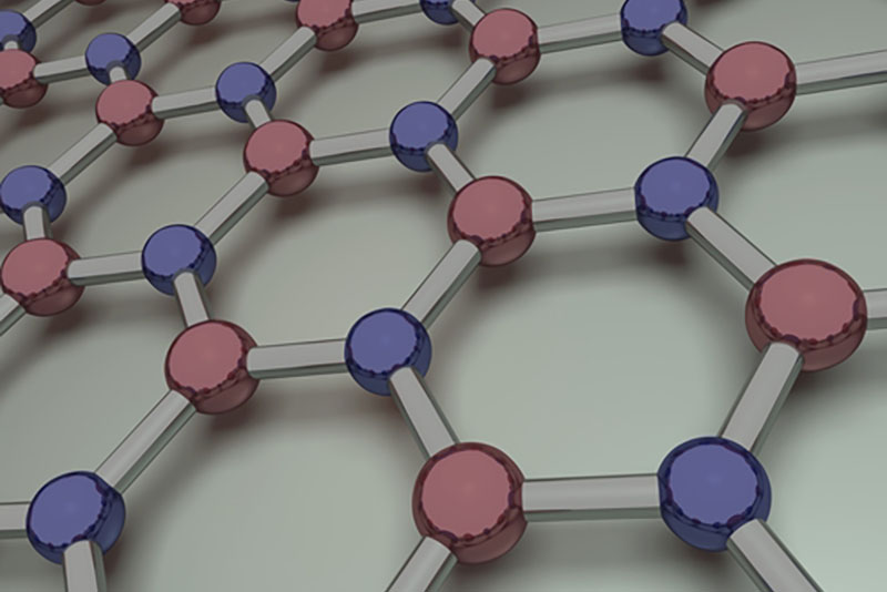
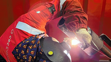
The commercial development of graphene-based electronics has been hampered by difficulties in growing the material directly onto dielectric substrates. Graphene’s unique electronic structure results from the sp2 hybridisation of carbon orbitals, combined with an open, 2D, hexagonal atomic arrangement. This can produce an exceptionally high charge carrier mobility, but only when grown on a smooth, chemically inert and electrically insulating substrate. Unfortunately, commonly used dielectric materials, such as silicon-based oxides and nitrides, tend to have rough surfaces and high dopant concentrations, as well as poor electronic and thermal transport properties, which make them unsuitable substrates for graphene growth.
Hexagonal boron nitride (h-BN) has been proposed as an alternative substrate material and exhibits superior physical characteristics and chemical stability compared to silicon-based substrates. Large-area coatings of h-BN have already been produced by chemical vapour deposition (CVD) methods, which involves the decomposition of boron nitride precursors over catalytic metal surfaces.
However, deposited h-BN must be transferred from the catalyst to a final dielectric substrate, and the wet/dry transfer processes involved can create surface corrugations and introduce impurities. The deposition process is also complex, requiring electrochemical or chemical-mechanical polishing steps, as well as high-temperature annealing.
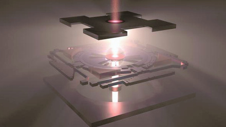
In December 2022, Globalwafers Co., Ltd. and The Board of Trustees of the University of Illinois, USA, were granted a European patent EP3455874B1 entitled Direct formation of hexagonal boron nitride on silicon based dielectrics. This patent describes a method of forming a multilayer structure including, in order, a single-crystal semiconductor wafer, a silicon nitride layer, a h-BN layer and a metal film. The h-BN layer is grown directly on the silicon nitride layer using low-pressure CVD (LPCVD), at a pressure below 250Torr and at a temperature of at least 1,000°C.
According to the patent, the inventors have identified a growth mechanism for h-BN that enhances the quality of the material deposited on silicon-based dielectric surfaces (thus avoiding the need for a metal catalyst, as well as associated pre-treatment and transfer steps), and improves the electrical transport properties of final graphene/h-BN heterostructures.
In particular, the inventors find that when the LPCVD process is carried out as claimed using boron- and nitrogen-containing reactant gases or vapours over a silicon nitride surface, a large-area and continuous thin film of h-BN can be formed by the interaction between (BN)XHY radicals and the N-terminated (1 0 0) Si3N4/Si surface.
Once the h-BN layer has been coated with a catalytic metal film, carbon can be caused to diffuse through the metal (for example, by exposing the multilayer structure to carbon-containing gas at elevated temperatures) to the h-BN/metal interface, at which a layer of graphene should precipitate on cooling.
The inventors find that an all-CVD growth process produces an h-BN layer with 3.4 times reduced roughness in comparison to the underlying Si₃N₄/Si surface. A graphene monolayer deposits on this surface exhibiting an enhanced intrinsic charge carrier mobility of 1,200cm2/Vs, in contrast to a mobility of 400cm²/Vs measured for graphene grown directly on Si3N4/Si.
The patent also describes how the inventors have verified their model for h-BN film growth kinetics using atomistic molecular dynamics simulations. In particular, they have modelled the adsorption of borazine (B3H6N3) molecules on SiO2/Si and Si3N4/Si surfaces and have found higher rates of single-molecule adsorption over (0 0 1) SiO2/Si due to an attractive negative surface charge caused by dangling oxygen atoms (compared to an electrically neutral (0 0 1) Si3N4/Si surface).
Clusters of borazine molecules then tend to attach to already-adsorbed molecules, so that overall adsorption to the SiO2/Si surface is more rapid due to the higher number of available attachment sites.
This suggests that molecular surface adsorption is the rate-limiting step in h-BN nucleation on Si-based dielectric surfaces and explains why much thicker h-BN films have been found to grow more rapidly on SiO₂ compared to Si3N4. The mechanism was also verified by experiments comparing growth rates over bare Si and O₂-plasma treated Si under the same CVD conditions. According to the inventors, this explains why thinner, smoother, h-BN films are formed over Si3N4/Si substrates.
Benefits of the claimed manufacturing method, according to the inventors, include versatility, scalability and compatibility with current semiconductor industry processes. They envisage use of the method to produce intelligently designed 3D heterostructures with applications including nanoscale electronics, energy conversion and optoelectronics.
Read the full patent at https://bit.ly/428E2y3