Additive manufacturing at sub-micrometre scale
A patent for an additive manufacturing process capable of producing sub-micrometre-scale features.
Additive manufacturing encompasses a variety of processes for constructing 3D objects by depositing, joining or fusing material. Common techniques include material jetting or extrusion, powder-bed fusion and directed energy deposition. The approach selected depends on the material to be deposited and the desired characteristics of the final product.
Multiphoton or two-photon lithography is a particular photolithographic technique that enables fine-scale features to be 3D printed using polymers, ceramics and glasses.
In traditional photolithography, a photoresist material is patterned by exposure to a light shone through a photomask that contains the desired pattern. Areas of the photoresist exposed to light undergo chemical changes (e.g. polymerisation) and, subsequently, patterned and non-patterned material can be separated, for example, by preferential dissolving using a developer solution.
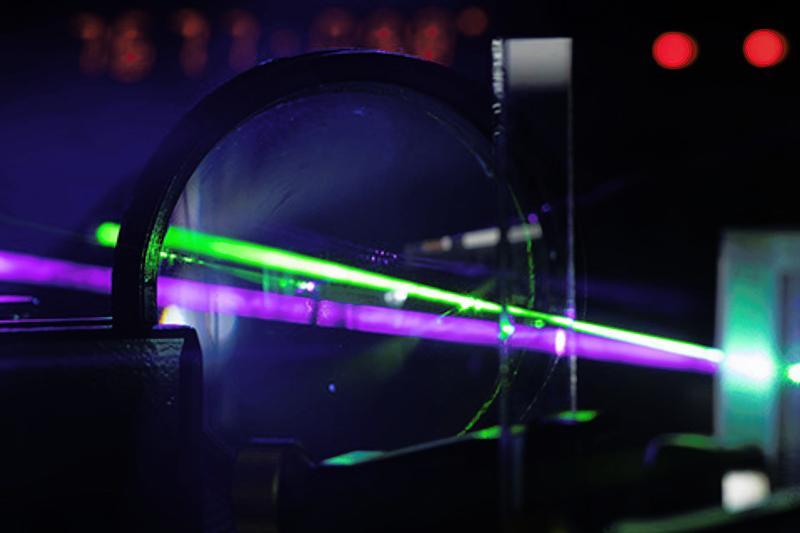
Multiphoton or two-photon lithography is based on the principle of two-photon absorption, whereby a molecule is excited by simultaneous absorption of two photons of identical or different frequencies.
The lithographic method uses a photosensitive material that is transparent at the wavelength of the exciting laser. However, by appropriate modulation of the laser light, two-photon absorption can be induced at the laser’s focal spot.
Importantly, the rate of two-photon absorption by a molecule varies with the square of the light intensity. While the rate of single-photon absorption is linear with respect to light intensity. The use of a focused, high-power laser, in which the light intensity is higher at the beam’s centre than at the periphery, enables fine control of patterning in two-photon absorption.
Two-photon additive manufacturing techniques are therefore able to produce arbitrary and complex 3D structures with sub-micrometre features, typically without the need for a photomask.
However, direct-write, two-photon, additive techniques suffer from low-processing rates (e.g. around 0.1mm3/hour). Attempts to increase the rate by parallelisation have previously been limited to generating arrays of identical features (rather than arbitrarily complex, non-periodic, 3D parts), or 2D parts with no depth resolvability.
European patent EP3732027B1, granted in February 2025 to Lawrence Livermore National Security, LLC, appears to describe a two-photon lithography system that dramatically increases processing rates, without adversely affecting the ability to fabricate complex 3D structures.
This is achieved by implementing a parallel illumination technique, in which an entire plane of around one million points is projected onto the photoresist material, rather than using the single-point illumination technique of existing commercial systems. According to the inventors, this enables the processing rate to be increased by at least a factor of 100.
The method described in the patent uses high-peak-power, pulsed laser sources (in particular, wideband, femtosecond pulsed lasers), in contrast to the incoherent sources used in standard micro-stereolithography. This ensures that nonlinear photo-absorption takes place over single-photon linear absorption.
In addition, the method uses a resist material that exhibits what is described as 'thresholding behaviour' – this means that a minimum nonlinear light-exposure dosage is required to induce a phase transition (e.g. from liquid to solid) in the material. Together, these aspects enable steep dosage gradients to be generated in the material during nonlinear absorption, and so features that are smaller than the diffraction-limited illumination spot can be generated.
According to the inventors, the method can simultaneously focus a collection of points, forming a projected image, in the interior of the resist material, without providing significant light intensity outside the focused depth. Moreover, the dosage at each individual focused spot can be tuned independently of the others.
By parallelising the formation of sub-micrometre features in this way, the processing rate is increased substantially and arbitrarily complex patterns can be created. This contrasts with conventional multiphoton lithography in which a laser beam is split into multiple focal spots with identical intensity distributions.
The patent also describes how the new method uses ‘temporal focusing’. In particular, the peak intensity during a laser pulse depends on both the beam’s spatial size and the pulse duration. According to the inventors, this means that a pulse’s intensity can be tuned independently by varying either parameter.
By focusing the beam using this technique, the inventors can achieve steep dosage gradients at a projected image plane, even when the projected image is large due to the presence of multiple focused spots.
A similar principle has previously been applied in fluorescence imaging of biomaterials and in material-removal-based fabrication processes. However, the inventors consider this to be the first successful application of the principle to multiphoton lithography.